For those that have dealt with high voltage remote control vehicle setups (Generally over 6s, 22.2V) the phenomenon of connector sparking (or arcing) is nothing new. Not only can this be frightening to the user, but it also causes the connector surface to become pitted, and over time the connector contact area will be reduced resulting in higher resistance. Thus, a connector that may have been originally rated for 60A may only be able to carry 40A before melting.
The reason for this arcing is the large ESC input capacitors. Under normal operation they serve as an electrical ‘buffer’, smoothing out current draw spikes generated by the motor under hard acceleration and temporary rotor field misalignment. Without them these currents would travel through the battery wires, generating large voltage spikes due to their inherent inductance. Obviously it is best to avoid large voltage spikes because they can exceed the ratings of components and cause failure.
However, the same ultra-high discharge qualities that make capacitors great as energy buffers, means that they also create huge currents when they voltage across their terminals changes. The goal of this post is to describe two different methods of reducing the inrush current and thereby preventing sparking when a battery and ESC are connected.
Method 1: Sequential Connection
The simpler of the two methods involves making two connections sequentially. The first connection involves a small resistor in series with the input capacitor. Those with some electrical knowledge will recognize this as an RC circuit. The capacitor charge time can then be controlled by the value of the resistor and capacitor.
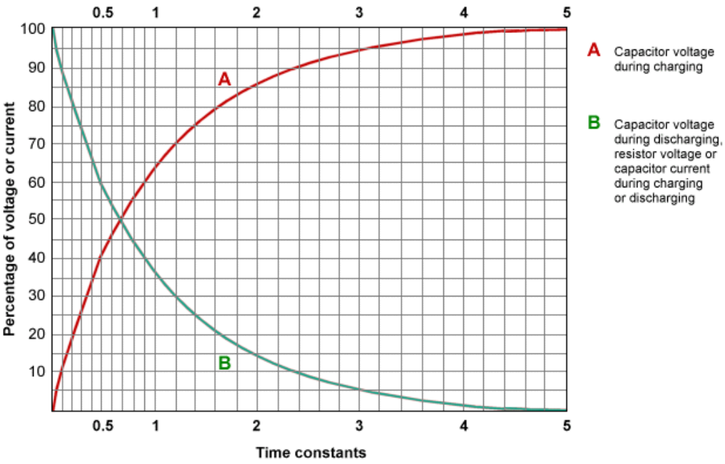
The peak current will depend on the size of input cap, but a good rule of thumb is that the capacitor should finish charging in about half a second. Looking at the graph, the capacitor is nearly finished charging at 4 time constants, thus 4*RC = 0.5s. Assuming a 1000uF input cap, a 120 ohm resistor is adequate.
At this point, the second connection is made, bypassing the resistor. We do this so that during normal operation, no extra resistance is introduced into the circuit.
Method 2: MOSFET Switching
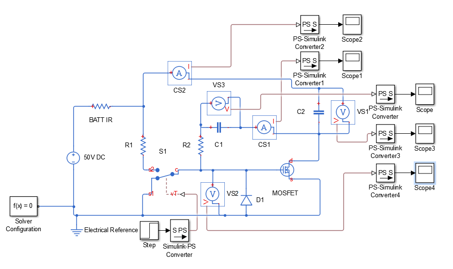
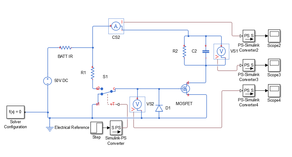
Where the previous method falls short, is that you always need to physically make the main power connection. Anti-spark connectors such as the XT-90S make this a little easier because the terminals are offset so that the capacitors are charged via the resistor circuit when the connector is partially inserted. However, for my next E-Vehicle project, I’d like to use a low current push button switch to turn on the electronics. This is only achievable through the use of a MOSFET. A MOSFET is a special type of transistor with characteristics that make it favourable for switching high currents, such as in motor drives. When a relative positive voltage of about 10V is applied to the gate of a MOSFET, it allows electricity to flow from its collector to emitter. However, unlike a BJT transistor in which the current is a function of gate current and current gain, the current across a MOSFET is only limited by the drain-source on resistance which is normally very low (a few milliohms). Thus, the power losses at high current remain relatively small. The application of a MOSFET in a inrush-current limiting circuit lies in its ability to also only be partially switched on. What I mean by this, is that by applying a voltage between 4V and 10V to the gate, the current across the collector and emitter can be regulated, thus slowly charging the input capacitors. Below, two different circuits are proposed. Both use the principle of capacitance to control the turn-on time of the MOSFET, although they accomplish it in different ways.
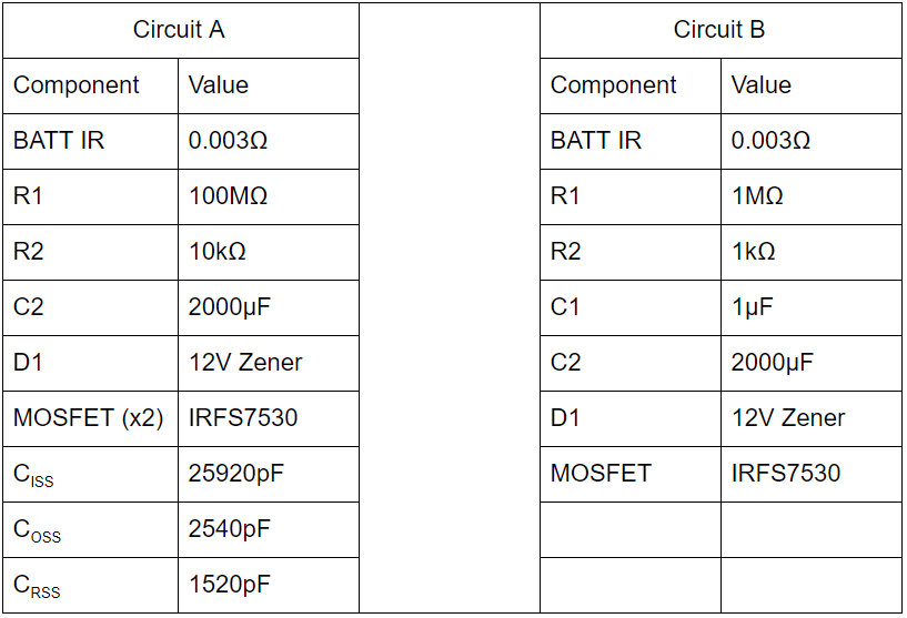
Circuit A:
External capacitor C1 is used as negative feedback to slowly charge MOSFET gate. As voltage is applied to gate, MOSFET opens and the capacitor is pulled down, resulting in gate current regulation.
Circuit B:
R1 and the internal capacitance of the MOSFET is used to create an RC circuit with a large time constant. The zener diode breaks down at 12V, thus the small portion of exponential decay is approximately linear.
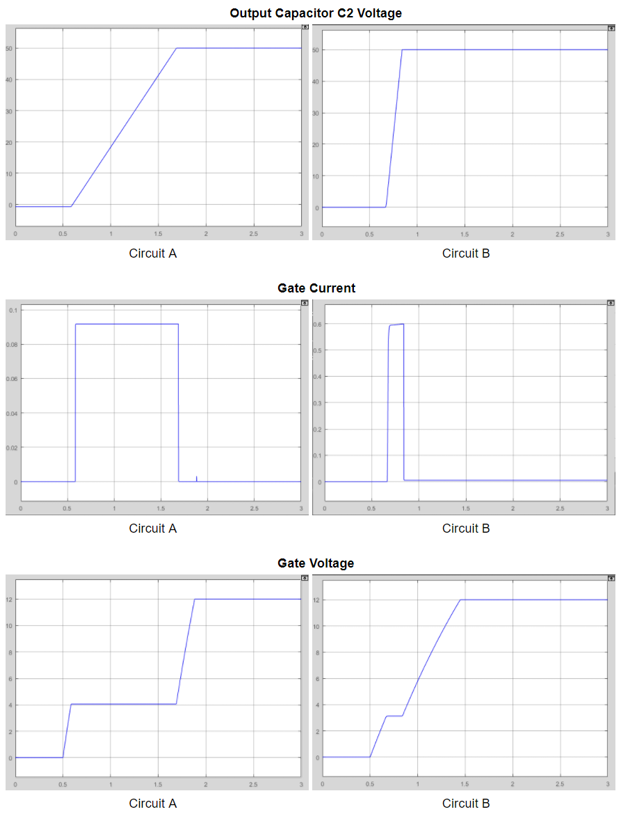
Simulink was used to run circuit simulations and graph various currents and voltages. The results are shown below.
Conclusion
- Both circuits exhibit approximately linear dv/dt on the output capacitor
- Charging rate can be managed by R1 (and C1 in circuit A)
- Circuit 2 requires higher value resistors; must consider humidity and PCB contamination
- Circuit 2 peak current (600mA) approaches safe dissipation power of MOSFET
For these reasons I have chosen to use circuit 1 to regulate gate turn-on time and consequently limit inrush current. To see how I have implemented these findings in my ongoing project, the e-Canoe, you can read the development update here.